Laboratory of Two-Dimensional Microelectronics Technology (№ 101)
101
Head of the Laboratory -
Dr. Sc. (Phys.-Math. Sciences), Professor A.V. Zotov
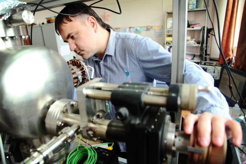
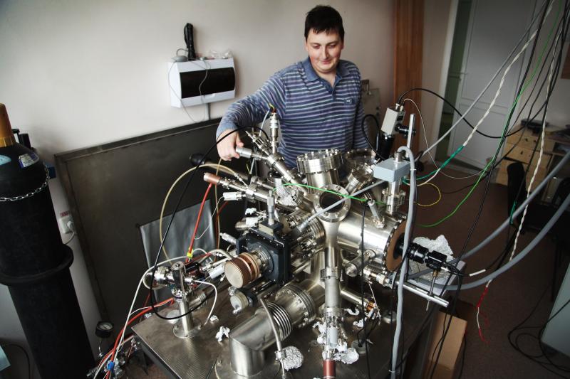
Staff
Total- 25,
Researchers - 14,
Dr. Sc. - 2,
PhD - 9.
Main research directions
- Investigation of the formation processes of the ordered nanostructures and low-dimensional structures on semiconductor surfaces.
- Determination of the electrical characteristics and other physical properties of the grown nanostructures.
- Theoretical simulations of the structure and properties of the nanostructures.
Principal results
- Possibility of modification of the Si(100)4×3-In nanocluster was found. The modification as a result of desired doping (formation of doped nanocluster) leads to changing of its electronic properties [Physical Review Letters, 2003]. The dynamic characteristics of the doped nanocluster have been studied. It was shown that the nanoclusters are a promising memory element for nanoelectronics [Physical Review B, 2006, Physical Review.B, 2007].
- Formation of ordered nanostructures in the submonolayer Cu/Si(111) system was investigated. Conductivity of ordered copper nanowires was studied. The nanowires were formed on the Cu/S1(111)’5×5’ surface as a result of self-assembly of the copper atoms. The surface demonstrates metallic conductivity, but it has strongly pronounced anisotropy. The Cu nanowires resistivity has been estimated [Nanotechnology, 2008]
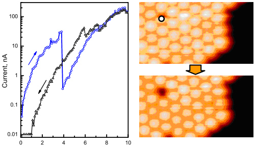
- Possibility of manipulation of a desired C60 fullerene laying in the close-packed array of the molecules on the (Au,In)/Si(111) surface using the scanning tunneling microscopy tip was studied. It was found that the removal of a fullerene (vacancy formation) as well as the shifting of a C60 molecule can be carried out in a wide range of the voltage, currency and power. Thus, the manipulation is not a result of any electronic effect, but it has entirely mechanical nature [Nanotechnology, 2013].
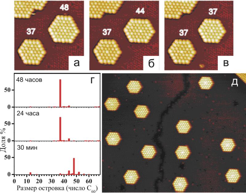
- Self-assembly of fullerene islands mediated by the moiré interference between an island and the underlying lattice has been studied. We have shown that this discovery suggests an unexplored tactic of engineering atomic scale moire magnifiers to facilitate the growth of monodisperse mesoscopic structures [Nature Communications, 2013].
Representative publications
- K. Oura, V.G. Lifshits, A.A. Saranin, A.V. Zotov, M. Katayama (Invited Review) Hydrogen interaction with clean and modified silicon surfaces. Surface Science Reports, 1999, 35(1-2), 1-74.
IF = 14.765
- A.A. Saranin, A.V. Zotov, V.G. Kotlyar, T.V. Kasyanova, O.A. Utas, H. Okado, M. Katayama, K. Oura Ordered arrays of Be-encapsulated Si nanotubes on Si(111) surface. Nano Letters, 2004, V.4, №8, P.1469-1473.
IF = 13.592
- D.V. Gruznev, A.V. Matetskiy, L.V. Bondarenko, O.A. Utas, A.V. Zotov, A.A. Saranin, M.Y.Lai, J.P. Chou, C.M. Wei, and Y.L. Wang. Stepwise self-assembly of C60 mediated by atomic scale moiré magnifiers. Nature Communications, 2013, Vol.4, Article number: 1679.
IF = 11.47
- V.G. Kotlyar, A.V. Zotov, A.A. Saranin, E.N. Chukurov, T.V. Kasyanova, M.A. Cherevik , I.V. Pisarenko, H. Okado, M. Katayama, K. Oura, V.G. Lifshits Doping of magic nanoclusters in the submonolayer In/Si(100) system. Physical Review Letters, 2003, V.91, P.026104-1-026104-4.
IF = 7.512
- M.Y. Lai, J.P. Chou, O.A. Utas, N.V. Denisov, V.G. Kotlyar, D.V. Gruznev, A.V. Matetsky, A.V. Zotov, A.A. Saranin, C.M. Wei, Y.L. Wang. Broken even/odd symmetry in self-selection of distances between nanoclusters due to presence/absence of topological solitons. Physical Review Letters, 2011, V.106, P.166101(4).
IF = 7.512
- Y.L. Wang, A.A. Saranin, A.V. Zotov, M.Y. Lai, H.H. Chang. Random and ordered arrays of surface magic clusters. International Reviews in Physical Chemistry, 2008, Vol.27, No. 2, P.317-360.
IF = 7.034
- L.V. Bondarenko, D.V. Gruznev, A.A. Yakovlev, A.Y. Tupchaya, D. Usachov, O. Vilkov, A. Fedorov, D.V. Vyalikh, S.V. Eremeev, E.V. Chulkov, A.V. Zotov & A.A. Saranin. Large spin splitting of metallic surface-state bands at adsorbate-modified gold/silicon surfaces. Scientific Reports, 2013, Vol.3, Article number: 1826
IF = 5.578
- D.V. Gruznev, L.V. Bondarenko, A.V. Matetskiy, A.A. Yakovlev, A.Y. Tupchaya, S.V. Eremeev, E.V. Chulkov, Jyu-Pin Chou, Ching-Ming Wei, Ming-Yu Lai, Yuh-Lin Wang, A.V. Zotov & A.A. Saranin. A strategy to create spin-split metallic bands on silicon using a dense alloy layer. Scientific Reports, 2014, Vol.4, Article number: 4742
IF = 5.578
9. D.A. Tsukanov, M.V. Ryzhkova, D.V. Gruznev, O.A. Utas, V.G. Kotlyar, A.V. Zotov, A.A. Saranin. Self-assembly of conductive Cu nanowires on Si(111)’5´5’-Cu surface. Nanotechnology, 2008, Vol. 19, P.245608-5.
IF = 3.821
- Dmitry A Olyanich, Vasily G Kotlyar, Tatiana V Utas, Andrey V Zotov and Alexander A Saranin. The manipulation of C60 in molecular arrays with an STM tip in regimes below the decomposition threshold. Nanotechnology, 2013, Vol.24, P.055302-8.
IF = 3.821